Hotline:400-857-8882
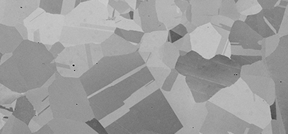
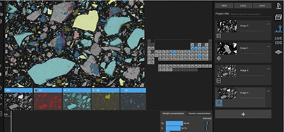
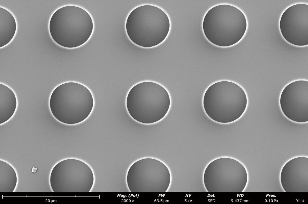
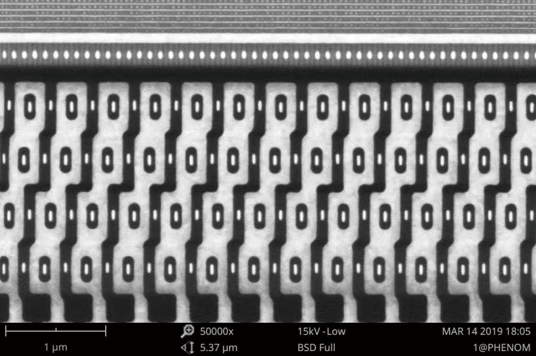
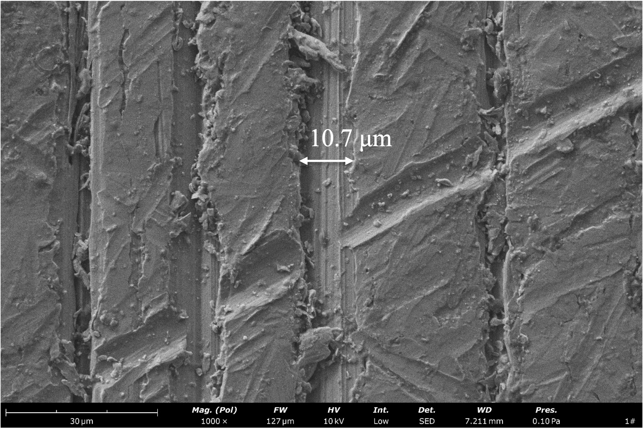
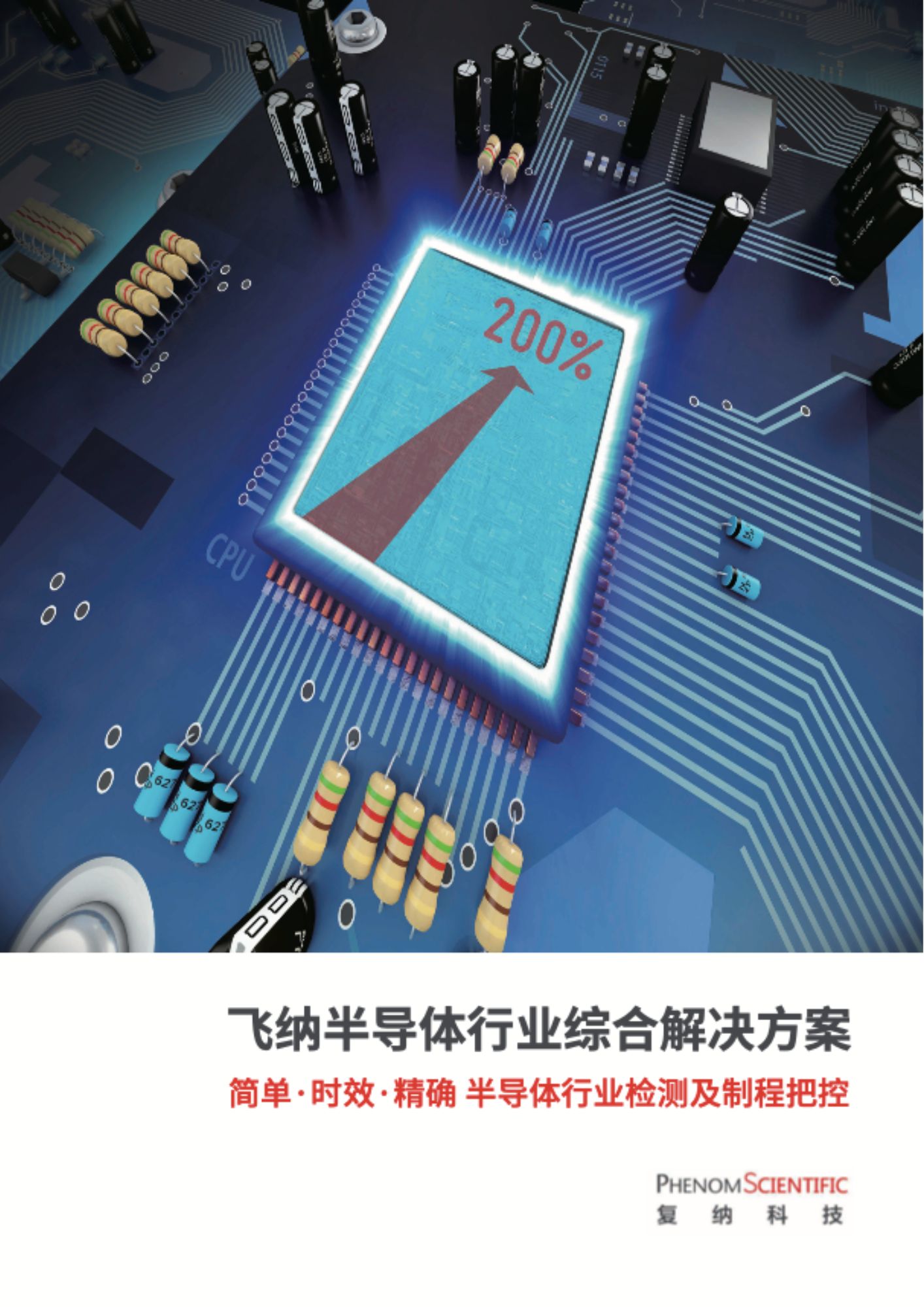
Semiconductor materials have always been the 'cornerstone' of chip manufacturing, serving as an important foundation for driving innovation in the integrated circuit industry. Phenom SEM can meet diverse material testing requirements and complex process controlments, providing a simple, efficient and accurate semiconductor inspection solution.

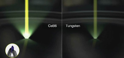
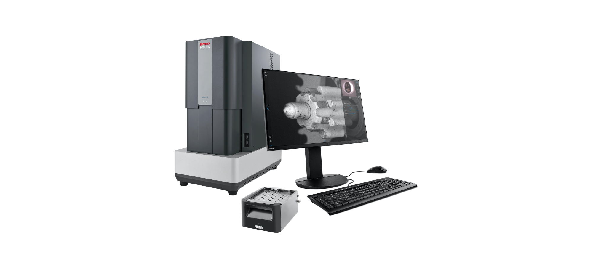
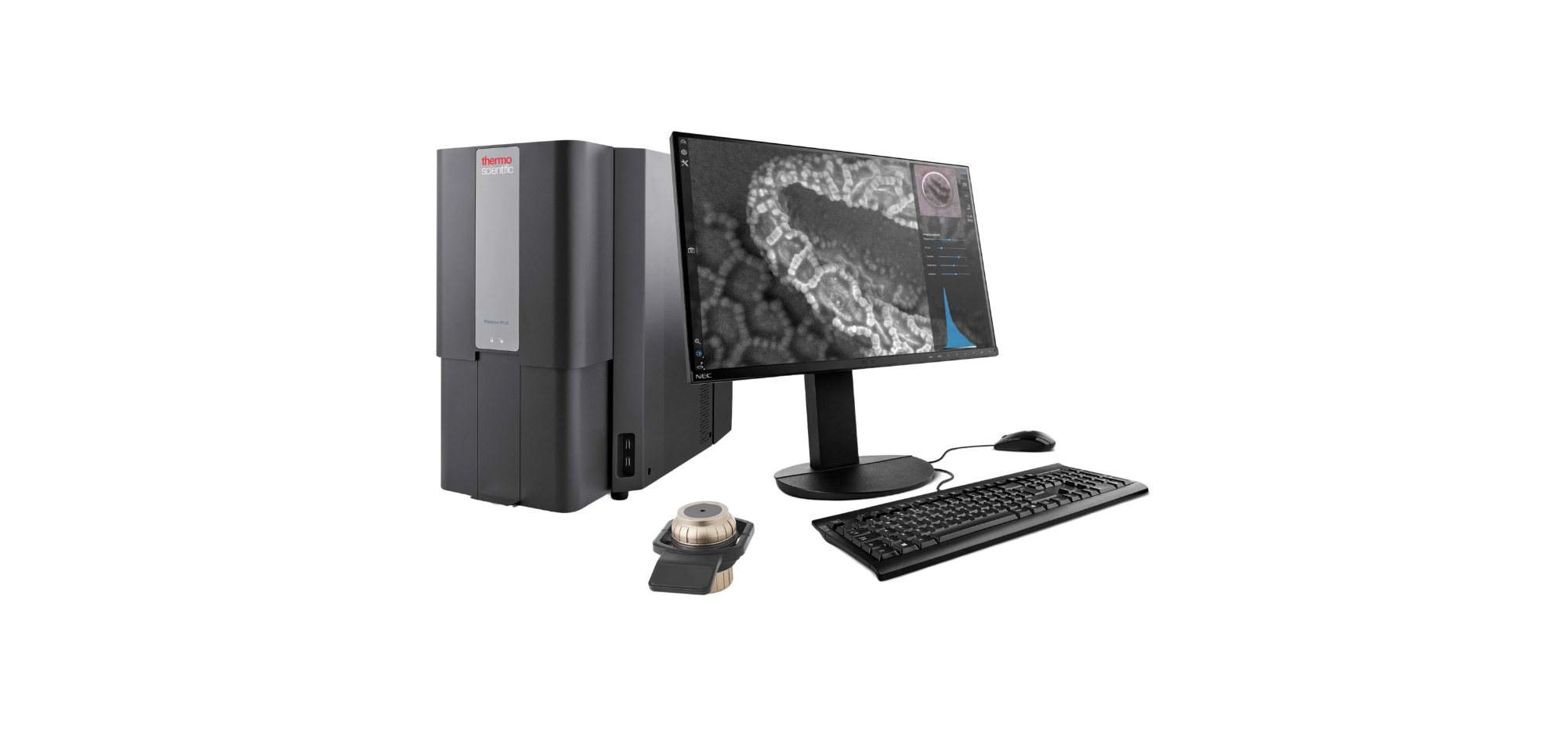
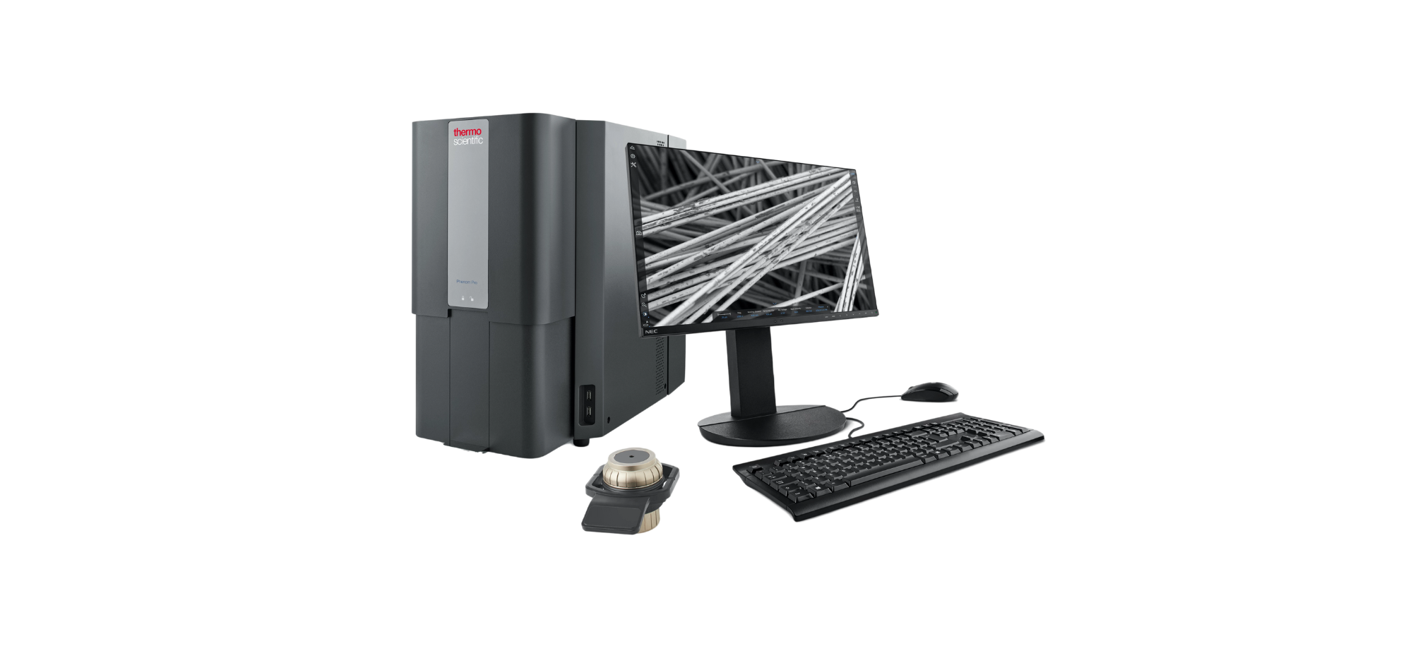
Phenom desktop SEM feature patented anti-vibration technology and can be placed in various environments, such as FA lab, high-rise office buildings, even next to production lines, allowing on-site sampling and observation.
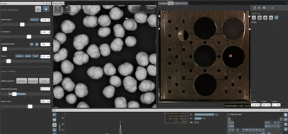
Load samples in one step, evacuate in 15 seconds, and achieve images in 30 seconds. Helpful in fast sample filtering, analysis position and the sample's pre-processing result confirming
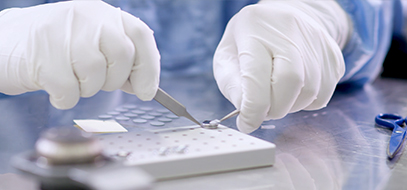
Simplifies the sample preparation process and suitable for various types of semiconductor materials.
PCB 行业产品分析与检测线上研讨会
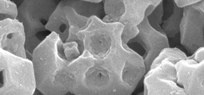
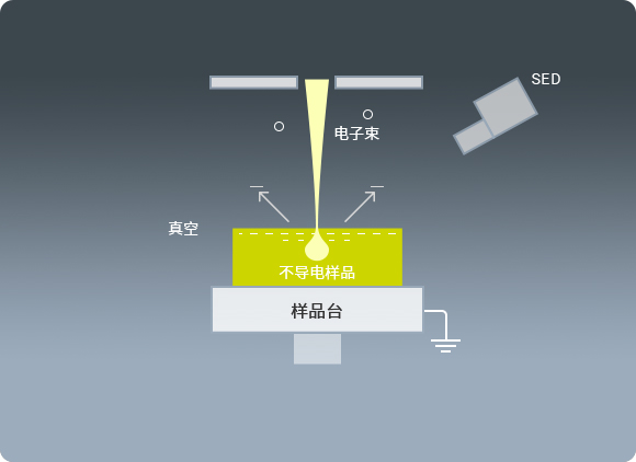
在进行电子器件失效分析时,首先观察失效件表面的微观形貌
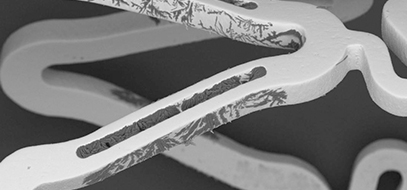
电子器件失效的原因千千万,其中引线框架表面的氧化状态,对器件的焊接有直接的影响。铜基框架表面接触氧气和水气,极容易被氧化,对后期器件焊接或者打线会产生负面的影响,所以需要关注框架铜表面的状态,借助扫描电镜(SEM)和能谱(EDS)抽检以保证品质极其重要。
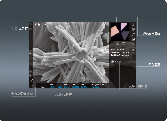
在进行电子器件失效分析时,首先观察失效件表面的微观形貌,飞纳台式扫描电镜集成有背散射(BSD,明暗衬度明显的成分像)和二次电子(SED,立体形貌像)两种成像模式,两种模式各有特点,可以呈现不同的细节信息。
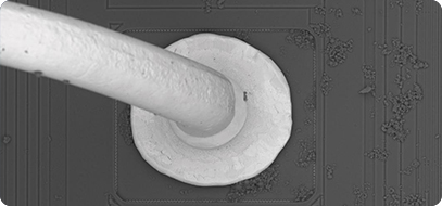
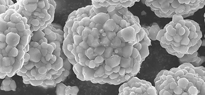
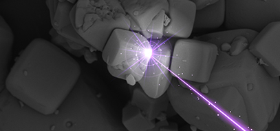
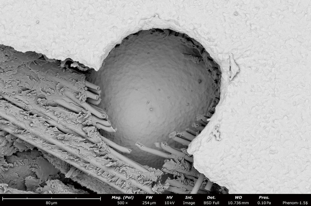
在电子器件的生产中,往往由于原料不纯、制程污染等原因引入一些杂质,这些异物对产品性能有很大影响,常会造成器件的失效。在分析的过程中,利用搭载 EDS 的扫描电镜的形貌分析能力和元素分析能力,可以很好的找到异物,并对异物形态、成分、位置进行确认,进而帮助异物的溯源和工艺的改善。如下述案例中所示为铝垫表面的异物分析,在光学显微镜下可以发现铝垫表面存在的一些白点,利用 Phenom 扫描电镜的光镜—电镜联动功能,可以快速的进行缺陷的定位,再通过 EDS-mapping 进行成分分析可以明显的发现含 Cl、Ag 的异物,残留的氯会导致打线的结合力变差而引起失效。
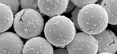
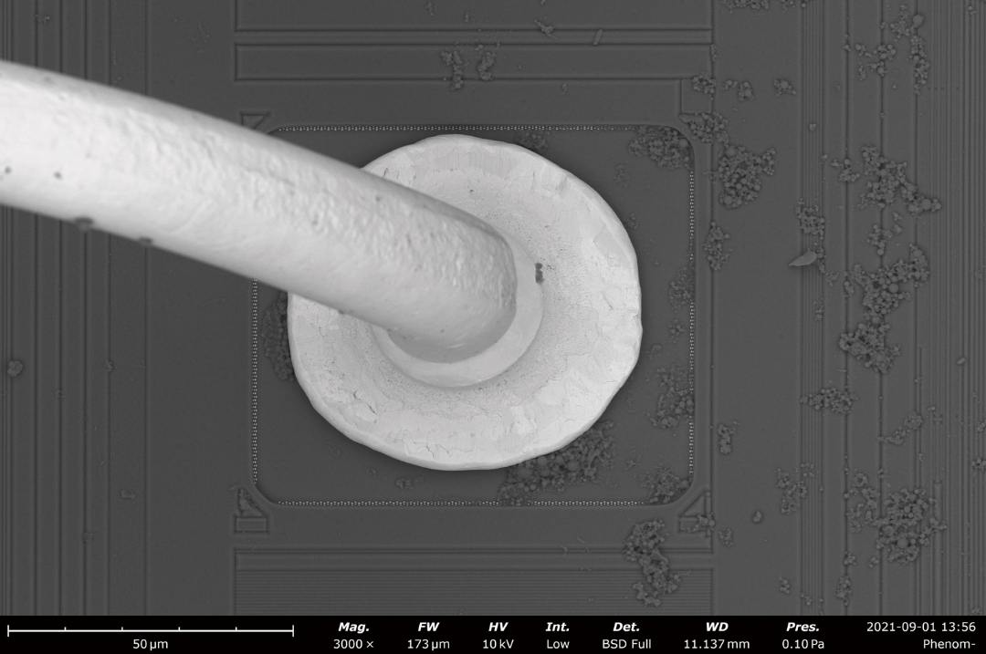
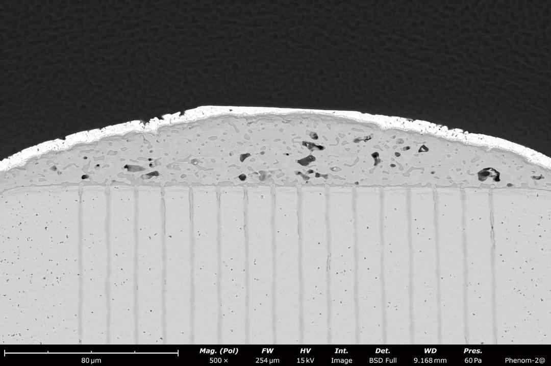
在制备过程中利用化镍金作为最后的保护层已经成为越来越多的电子产品的制备工艺了,但是化镍金的表面也有可能遇到吃锡不良的问题,金面污染和镍腐蚀就是两种典型的原因。如下案例中 (A)、(B) 所示,在金面上 EDS 分析发现了明显的 C、O、S 等杂质元素,这些污染物就会导致焊接过程中出现吃锡不良。另外一种吃锡不良的原因-镍腐蚀通过表面往往很难发现,这时可以借助离子切割获得平整的断面,对断面进行 EDS 分析就可以对是否是镍腐蚀造成吃锡不良进行分析了。

吃锡不良缺陷的 EDS 分析
If you want to learn more about product information, please fill out the following information to download the product manual. We will reply to you as soon as we receive your message.
隐私政策隐私政策隐私政策隐私政策隐私政策隐私政策隐私政策隐私政策隐私政策隐私政策隐私政策隐私政策隐私政策隐私政策隐私政策隐私政策隐私政策隐私政策隐私政策隐私政策隐私政策
隐私政策隐私政策隐私政策隐私政策隐私政策隐私政策隐私政策隐私政策隐私政策隐私政策隐私政策隐私政策隐私政策隐私政策隐私政策隐私政策隐私政策隐私政策隐私政策隐私政策隐私政策隐私政策隐私政策隐私政策隐私政策隐私政策隐私政策隐私政策隐私政策隐私政策隐私政策隐私政策隐私政策隐私政策隐私政策
隐私政策隐私政策隐私政策隐私政策隐私政策隐私政策隐私政策隐私政策隐私政策隐私政策隐私政策隐私政策隐私政策隐私政策隐私政策隐私政策隐私政策隐私政策隐私政策隐私政策隐私政策隐私政策隐私政策隐私政策隐私政策隐私政策隐私政策隐私政策隐私政策隐私政策隐私政策隐私政策隐私政策隐私政策隐私政策
隐私政策隐私政策隐私政策隐私政策隐私政策隐私政策隐私政策隐私政策隐私政策隐私政策隐私政策隐私政策隐私政策隐私政策隐私政策隐私政策隐私政策隐私政策隐私政策隐私政策隐私政策隐私政策隐私政策隐私政策隐私政策隐私政策隐私政策隐私政策隐私政策隐私政策隐私政策隐私政策隐私政策隐私政策隐私政策隐私政策隐私政策隐私政策隐私政策隐私政策隐私政策隐私政策隐私政策隐私政策隐私政策隐私政策隐私政策隐私政策隐私政策隐私政策隐私政策隐私政策隐私政策隐私政策隐私政策隐私政策隐私政策隐私政策隐私政策隐私政策隐私政策隐私政策隐私政策


Email : info@phenom-china.com
Address:Room 705, T5 Lihpao Plaza,No.88Shenbin Road,Hongqiao, Shanghai,P.R.China
Email : info@phenom-china.com
Address:Room 118, Block A, W.4th Ring Road North No.119 Siji Huigu Numeral Industrial Park, Haidian, Beijing, P. R. China
Email : info@phenom-china.com
Address:Unit 601-602, Block C, Luoxuan Avenue No.87, Haizhu,
Guangzhou, Guangdong, China
Email : info@phenom-china.com
Address:Block C No.106, Jinyun East 3rd Alley Finance Cornfield,
Chengdu, Sichuan, China


@ 2022 复纳科学仪器(上海) 有限公司 飞纳电镜 版权所有 沪ICP备12015467号-1